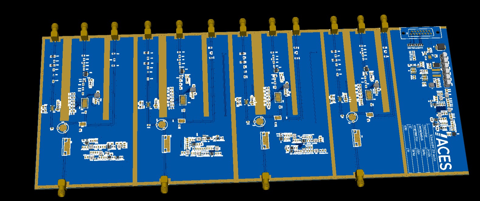
High-Speed Digital PCB Design
At Zaenex, we deliver RF and High-Speed Digital PCB Designs that set new standards for performance, signal integrity, and reliability in complex multi-channel systems.
- Impedance Control: Precise layer stack-up design to maintain target impedance (typically 50Ω) within ±5% tolerance.
- Crosstalk Mitigation: Optimized routing and spacing strategies ensuring FEXT below 3%.
- Differential Pair Routing: Tight trace length matching (≤ 5 mils) and phase skew control (≤ 10 ps) for noise immunity.
- Power Integrity (PI): Strategic decoupling and low-inductance power planes for stable delivery.